
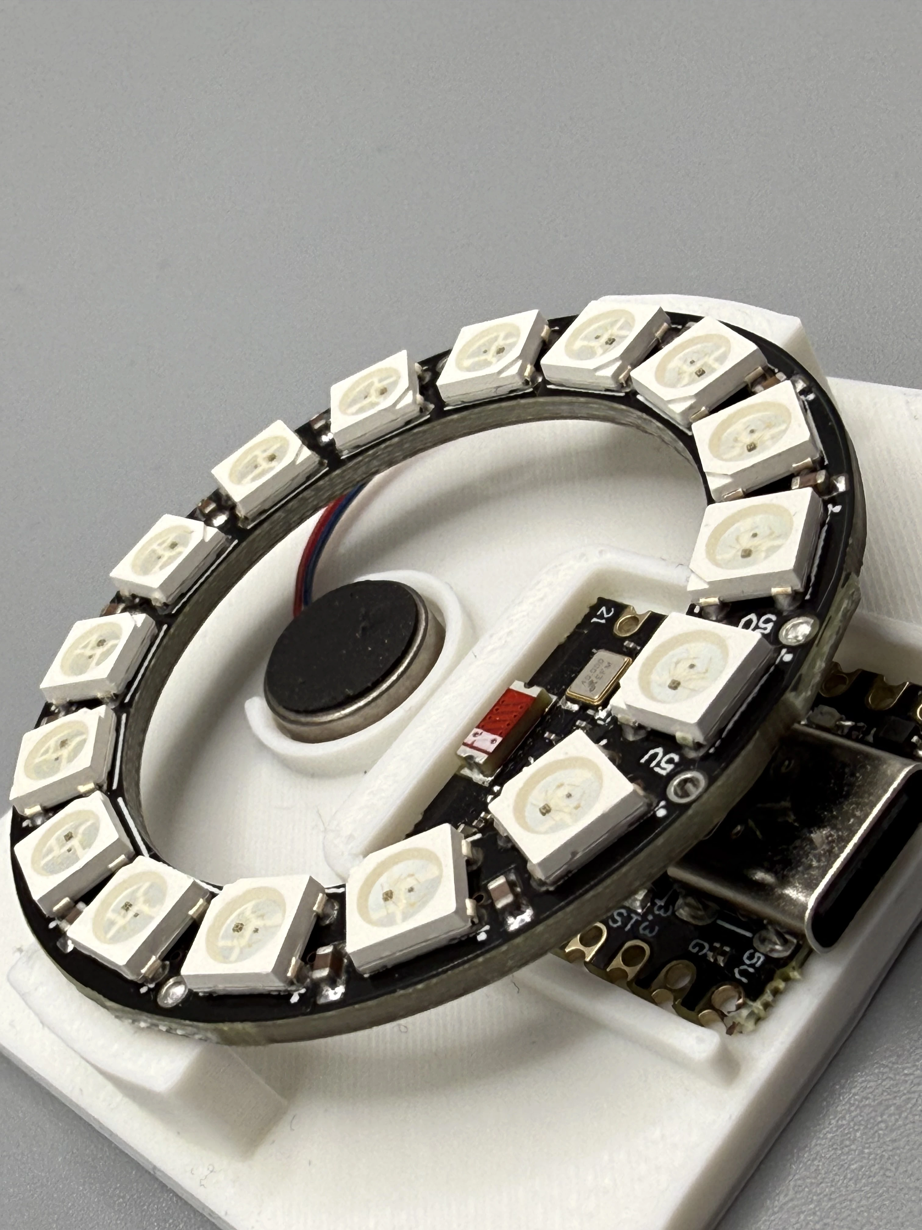
Hands-On Prototype
Development initiated with a structural alpha prototype focused on validating basic driving algorithms and circuit paths. Aggressive verification benchmarks isolated current consumption leakages and established stable firmware foundations prior to hardware finalization loops.
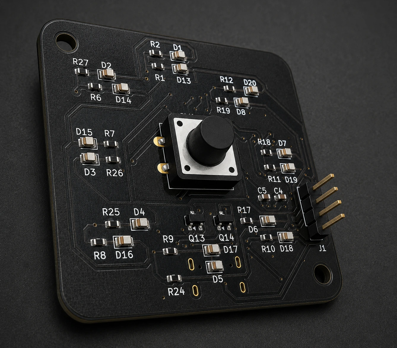
PCB Optimization & Layout
Migrating structural proof vectors into a manufacturing-ready multi-layer ecosystem. Path trace structures were refined to eliminate component footprints, lowering component bill of materials (BOM) values down to a target parameters envelope while supporting a clean, circular surface mount display interface.
Enclosure Development and Integration
The complete product enclosure assembly cycle was engineered for flawless structural handshakes. Mechanical mounting profiles were re-designed to drop manual production requirements from 15 minutes down to an agile 30-second snap-fit layout, optimized directly for rapid scaling.